gpu architecture
ampere 100

a100 滴滴云
https://developer.nvidia.com/blog/nvidia-ampere-architecture-in-depth/
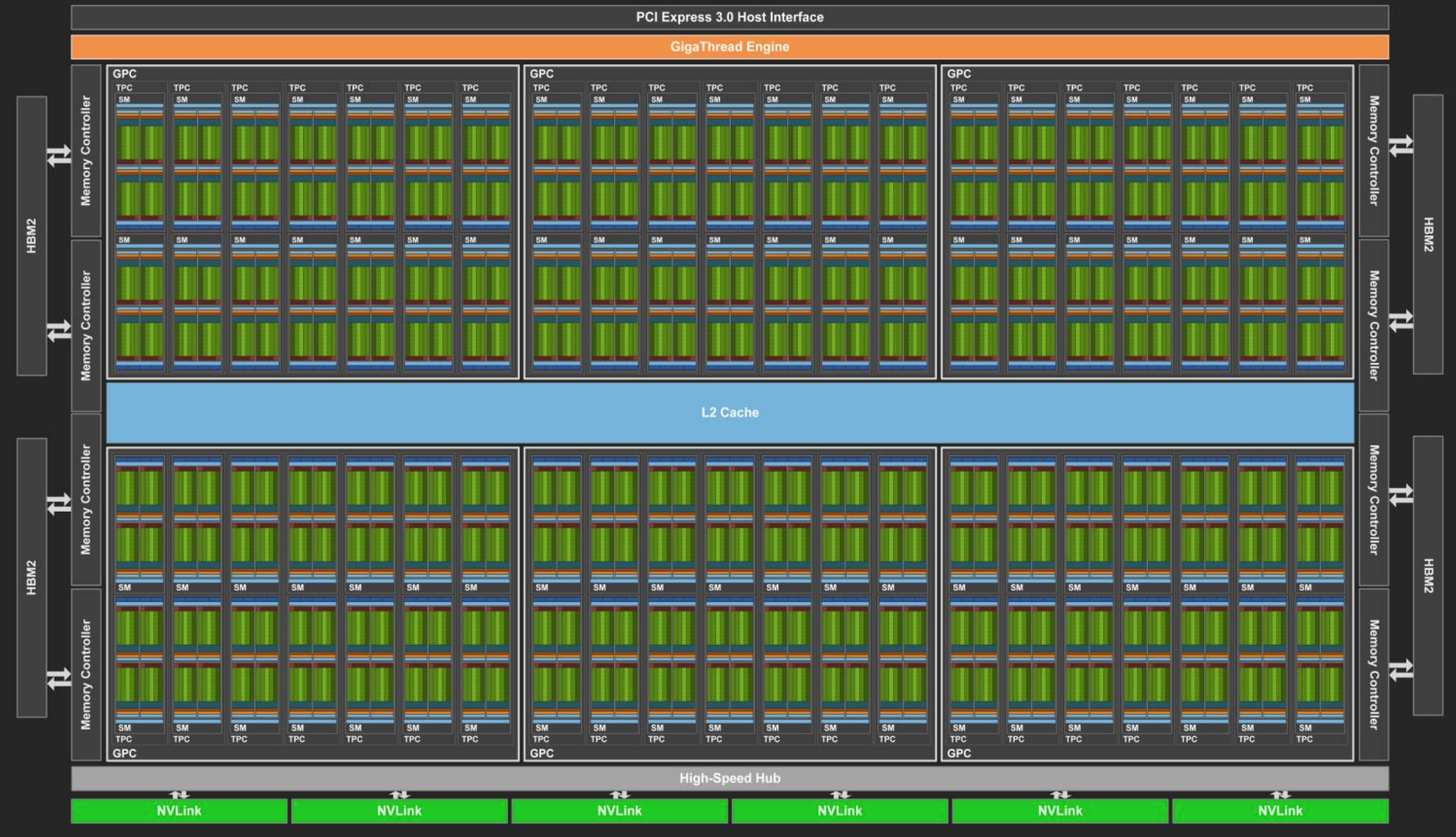
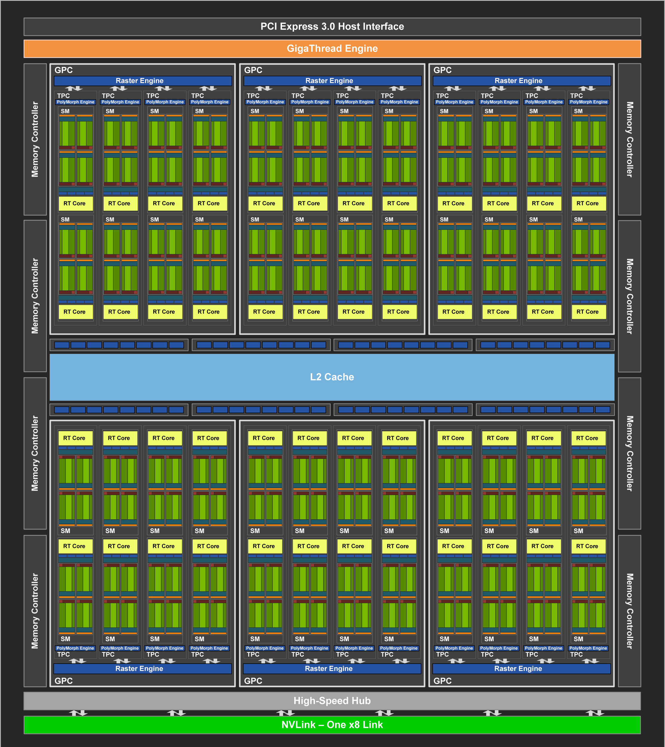
The full implementation of the GA100 GPU includes the following units:
- 8 GPCs, 8 TPCs/GPC, 2 SMs/TPC, 16 SMs/GPC, 128 SMs per full GPU
- 64 FP32 CUDA Cores/SM, 8192 FP32 CUDA Cores per full GPU
- 4 third-generation Tensor Cores/SM, 512 third-generation Tensor Cores per full GPU
- 6 HBM2 stacks, 12 512-bit memory controllers
five active HBM2 stacks, HBM2 1215 MHz(10 512-bit memory controllers, not full GA100),1555 GB/sec = 10 * 512 * 1215 * 2/8
Turing
| Brand Name | GPU Architecture | Tensor Core | NVIDIA CUDA® Cores | TensorFLOPS | Single-Precision | Double-Precision | Mixed-Precision(FP16/FP32) | INT8 | INT4 | GPU Memory | Interconnect Bandwidth | System Interface |
|---|---|---|---|---|---|---|---|---|---|---|---|---|
| V100 PCle | NVIDIA Volta | 640 1nd | 5,120 | 112 TFLOPS | 14 TFLOPS | 7 TFLOPS | 12x TFLOPS | 32 GB HBM2 900 GB/sec | 32 GB/sec | x16 PCIe Gen3 | ||
| V100 SXM2 | NVIDIA Volta | 640 1nd | 5,120 | 125 TFLOPS | 15.7 TFLOPS | 7.8 TFLOPS | 32 GB HBM2 900 GB/sec | 300 GB/sec | x6 NVLink 2.0 | |||
| T4 | NVIDIA Turing | 320 2nd | 2,560 | 8.1 TFLOPS | 65 TFLOPS | 130 TOPS | 260 TOPS | 16 GB GDDR6 300 GB/sec | 32 GB/sec | x16 PCIe Gen3 |
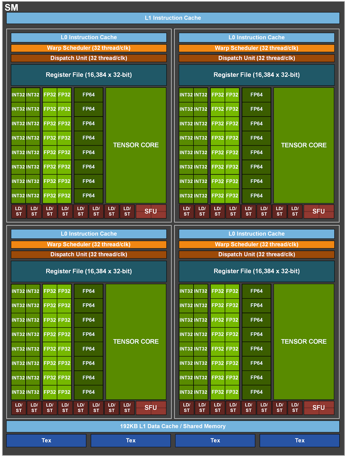
Nvidia Jetson
Orin 64GB
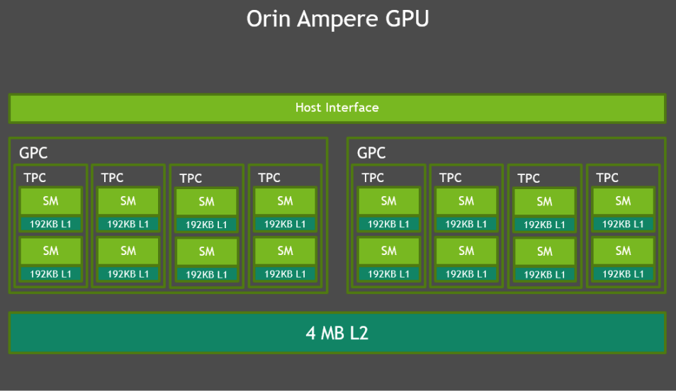
(2 * 4 * 2) * 4 = 64 Tensor Cores
(2GPC * 4TPC/GPC * 2SMs/TPC) * 128 = 2048 CUDA Cores (INT32+FP32)
int8算力
- 稀疏算力 Sparse TOPS
270 TOPS = 170T+105T(52.5*2), 其中Tensor Core贡献(1.3GHz * 64 * 256 * 2 * 2) * 2= 85 T * 2, int8是fp16两倍。 DLA 2.0 每个为52.5 TOPS sparse INT8 - 稠密算力 Dense TOPS
GPU Infos
P100
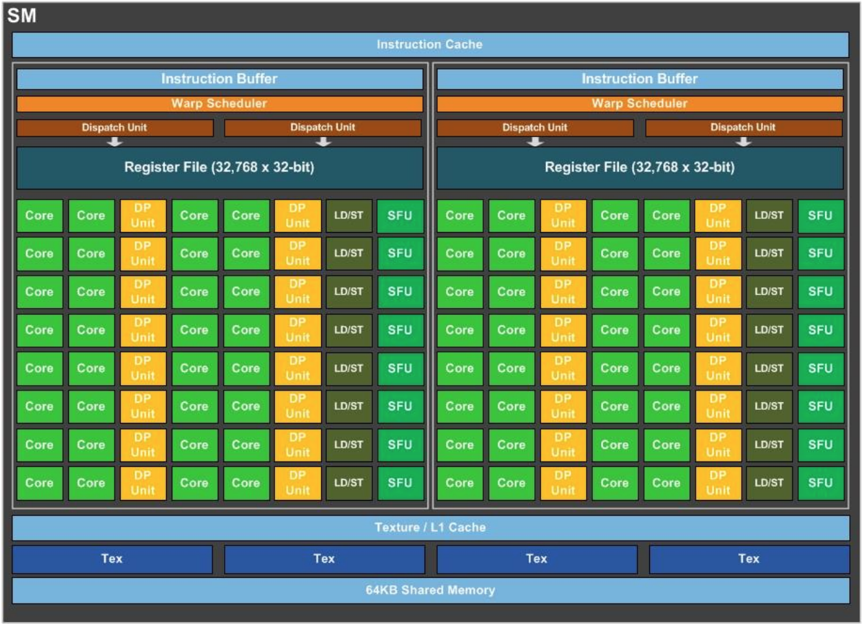
V100
- ALU
- 5376 FP32 cores = 6 GPC * 7 TPC * 2 SM * 64 FP32 cores(64 INT32 cores, 32 FP64 cores, 8 Tensor Cores, Four texture units)
- SM
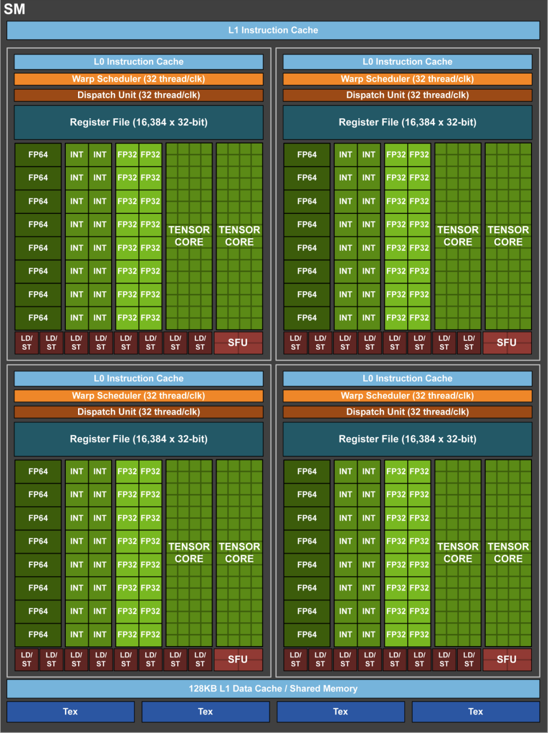
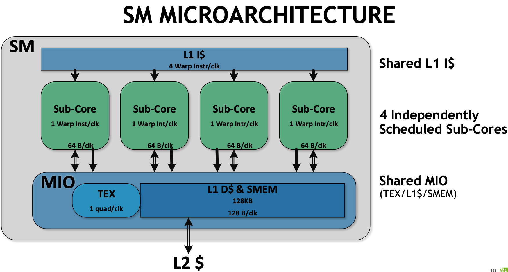
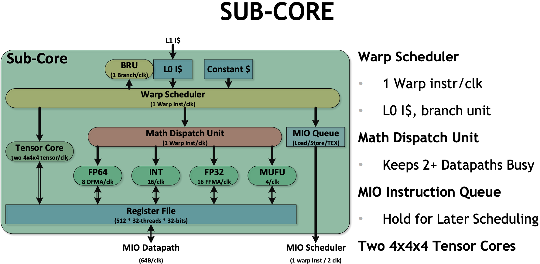
- 64 FP32 + INT32 cores, 32 FP64 cores, 8 tensor cores(FP32/FP16 mixed-precision)
- 4 subcore inside SM, 16 FP32 + INT32 cores, 8 FP64 cores, 2 tensor cores, 8 LD/ST units
- TensorCore: 64 floating point(FP16) FMA / (TensorCore *clock), 512 per SM per clock. 64 * 640 TensorCore * 2 * 1530 Mhz = 125 TFlops
- single precision (FP32) floating-point calculations: (5120 FP32 CUDA cores) × (2 flop/core/cycle) × (1.53 Gcycle/s) ≈ 15.7 Tflop/s, The factor of 2 flop/core/cycle comes from the ability of each core to execute FMA instructions(instruction throughput is N/32 instructions per clock cycle).
- Mem
- 512 bit * 8 memory controllers
- 6144 KB L2 cache
- IO
- six links and the bi-directional bandwidth of each link is 50 GB/s, so the bi-directional bandwidth between different GPUs is up to 300 GB/s.
- ALU
- T4
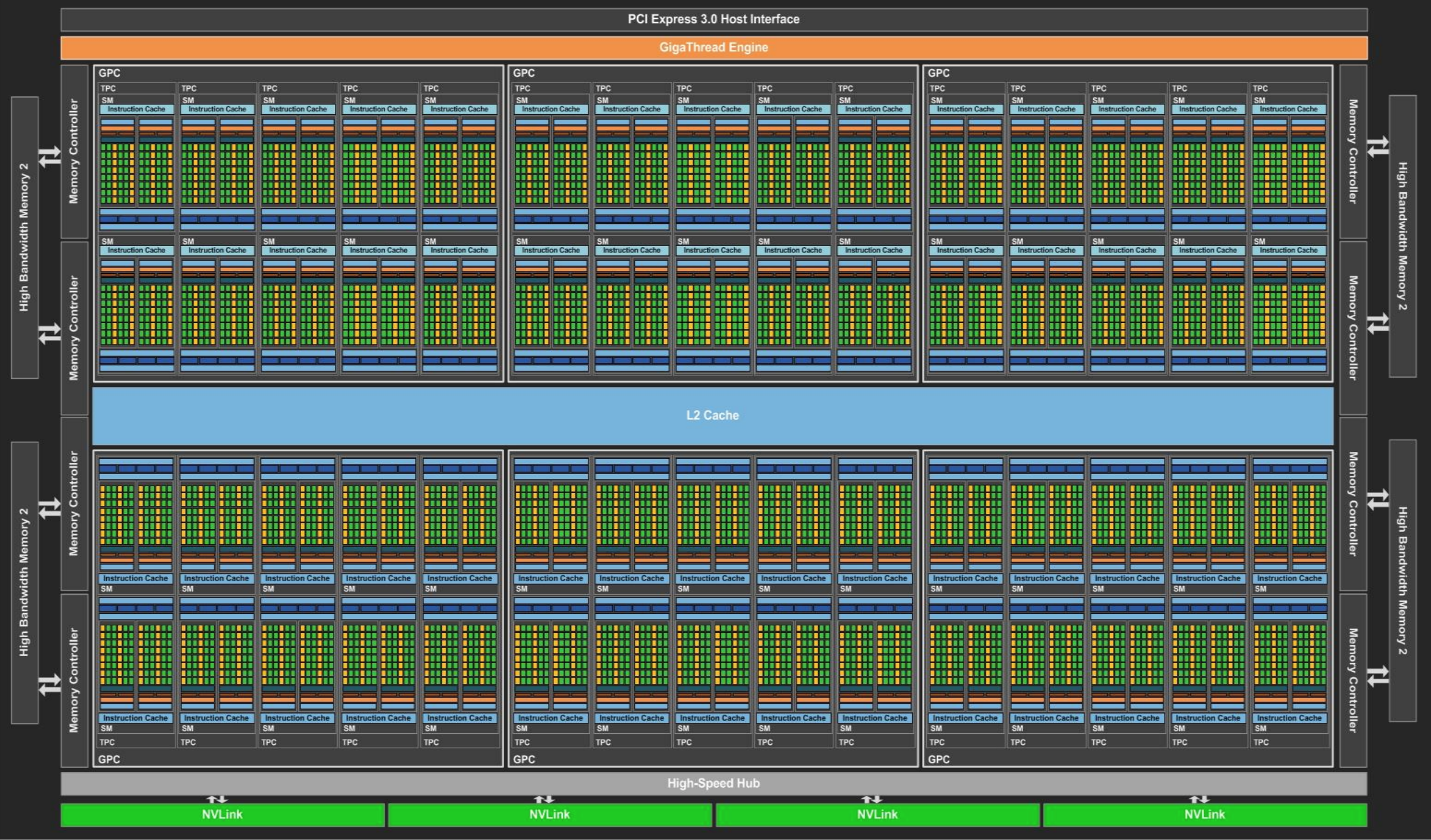
- A100
- ALU
- 8192 FP32 cores = 8 GPC * 8 TPC * 2 SM * 64 FP32 cores(64 INT32 cores, 32 FP64 cores, 4 Tensor Cores, Four texture units)
- SM
- 64 FP32 + INT32 cores, 32 FP64 cores, 4 * 3rd tensor cores(FP32/FP16, int8/int4 mixed-precision)
- 4 subcore inside SM, 16 FP32 + INT32 cores, 8 FP64 cores, 1 tensor cores, 8 LD/ST units
- TensorCore: 256 floating point(FP16) FMA / (TensorCore *clock), 256 * 4 * 108 * 2 * 1.41 Gcycle/s = 312 TFlops. Sparse performance double.
- single precision (FP32) floating-point calculations: (8192 FP32 CUDA cores) × (2 flop/core/cycle) × (1.41 Gcycle/s) ≈ 23.1 Tflop/s, The factor of 2 flop/core/cycle comes from the ability of each core to execute FMA instructions(instruction throughput is N/32 instructions per clock cycle).
- 108(7 * 8 * 2) * 64 * 1410 Mhz * 2 = 19.5 TFlops
- Mem/IO
- 512 bit * 12 memory controllers (Full A100), 512 * 10 (A100)
- 5 active HBM2 stacks, HBM2 1215 MHz(10 512-bit memory controllers, not full GA100),1555 GB/sec = 10 * 512 * 1215 * 2/8
- 192 KB shared-mem / L1 per SM
- 40 MB L2 cache
- NVLink: 50 Gbit/sec * 12 = 600 Gbit/sec
- ALU

- H00
https://www.nextplatform.com/2022/03/31/deep-dive-into-nvidias-hopper-gpu-architecture/
https://www.hpctech.co.jp/catalog/gtc22-whitepaper-hopper_v1.01.pdf
Comparison of NVIDIA Tesla GPUs
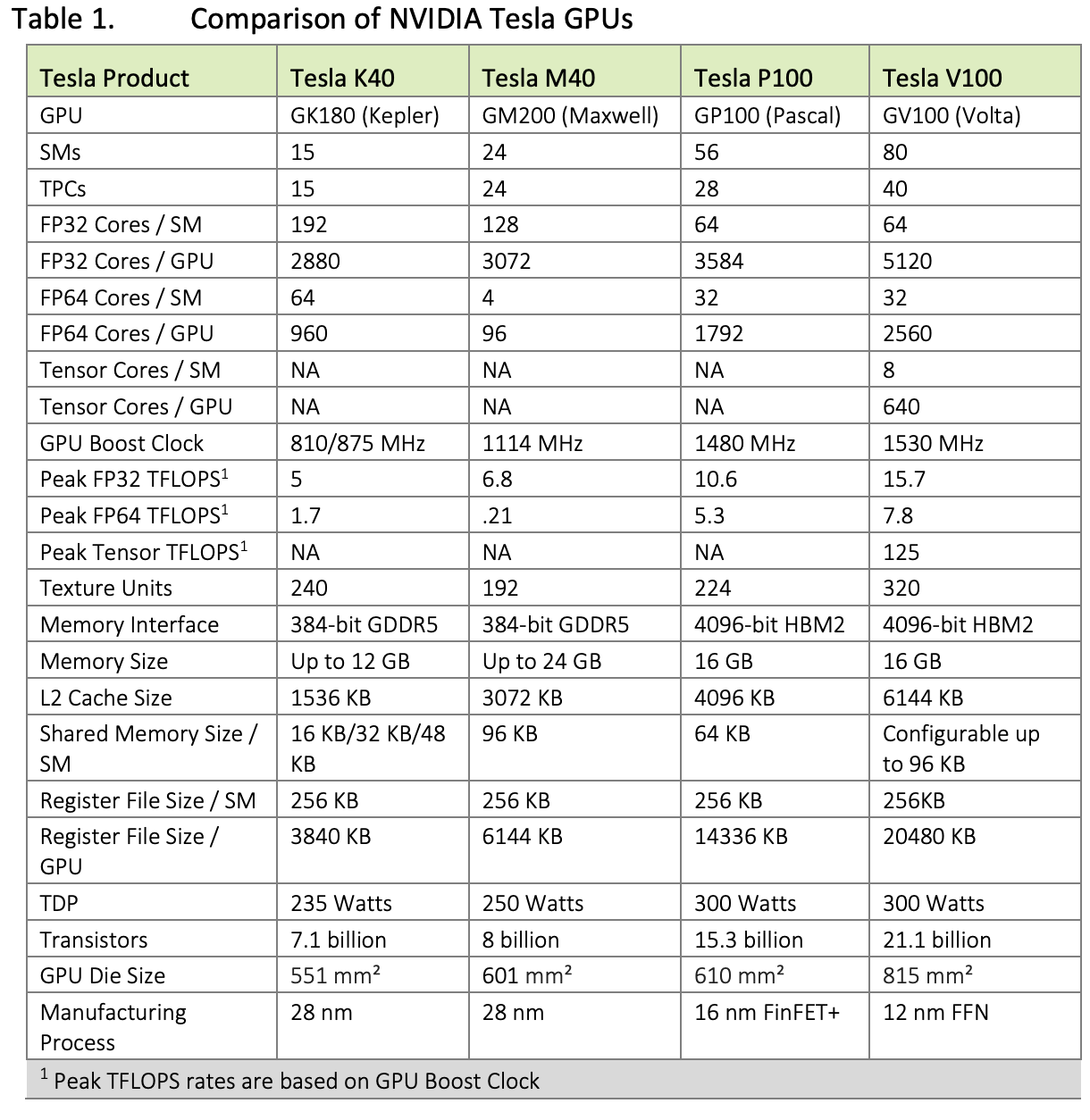
| Data Center GPU | NVIDIA Tesla P100 | NVIDIA Tesla V100 | NVIDIA A100 |
|---|---|---|---|
| GPU Codename | GP100 | GV100 | GA100 |
| GPU Architecture | NVIDIA Pascal | NVIDIA Volta | NVIDIA Ampere |
| GPU Board Form Factor | SXM | SXM2 | SXM4 |
| SMs | 56 | 80 | 108 |
| TPCs | 28 | 40 | 54 |
| FP32 Cores / SM | 64 | 64 | 64 |
| FP32 Cores / GPU | 3584 | 5120 | 6912 |
| FP64 Cores / SM | 32 | 32 | 32 |
| FP64 Cores / GPU | 1792 | 2560 | 3456 |
| INT32 Cores / SM | NA | 64 | 64 |
| INT32 Cores / GPU | NA | 5120 | 6912 |
| Tensor Cores / SM | NA | 8 | 42 |
| Tensor Cores / GPU | NA | 640 | 432 |
| GPU Boost Clock | 1480 MHz | 1530 MHz | 1410 MHz |
| Peak FP16 Tensor TFLOPS with FP16 Accumulate1 | NA | 125 | 312/6243 |
| Peak FP16 Tensor TFLOPS with FP32 Accumulate1 | NA | 125 | 312/6243 |
| Peak BF16 Tensor TFLOPS with FP32 Accumulate1 | NA | NA | 312/6243 |
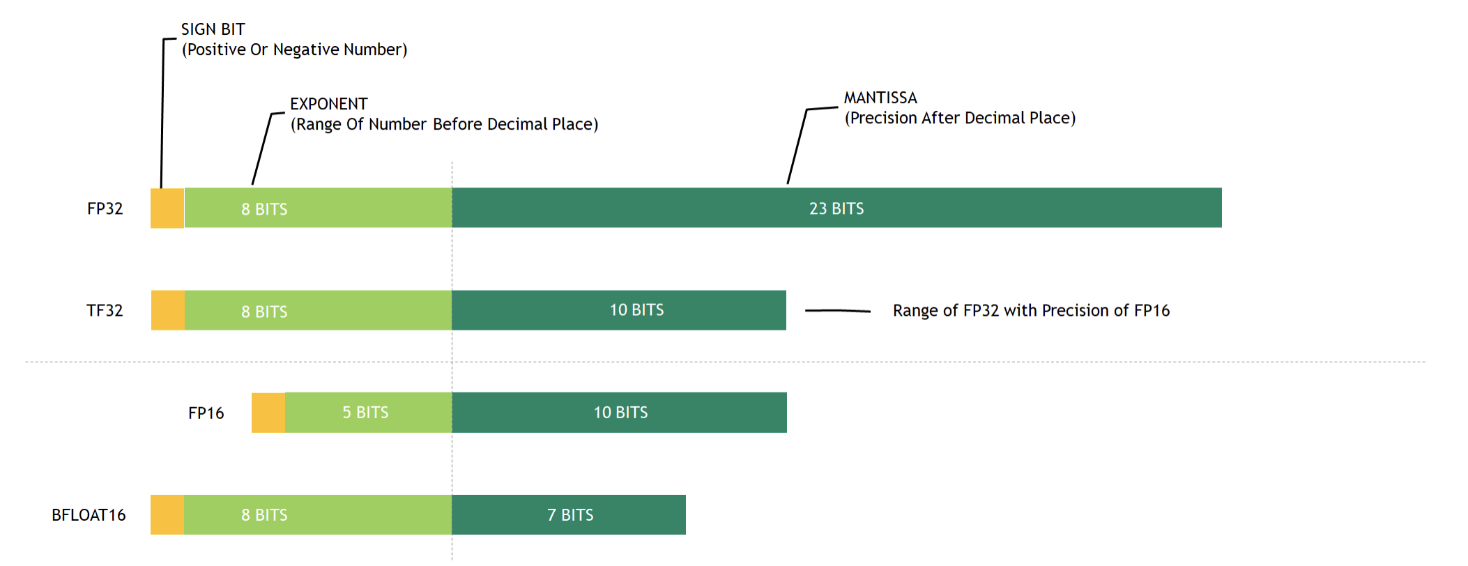
| Peak TF32 Tensor TFLOPS1 | NA | NA | 156/3123 |
| Peak FP64 Tensor TFLOPS1 | NA | NA | 19.5 |
| Peak INT8 Tensor TOPS1 | NA | NA | 624/12483 |
| Peak INT4 Tensor TOPS1 | NA | NA | 1248/24963 |
| Peak FP16 TFLOPS1 | 21.2 | 31.4 | 78 |
| Peak BF16 TFLOPS1 | NA | NA | 39 |
| Peak FP32 TFLOPS1 | 10.6 | 15.7 | 19.5 |
| Peak FP64 TFLOPS1 | 5.3 | 7.8 | 9.7 |
| Peak INT32 TOPS1,4 | NA | 15.7 | 19.5 |
| Texture Units | 224 | 320 | 432 |
| Memory Interface | 4096-bit HBM2 | 4096-bit HBM2 | 5120-bit HBM2 |
| Memory Size | 16 GB | 32 GB / 16 GB | 40 GB |
| Memory Data Rate | 703 MHz DDR | 877.5 MHz DDR | 1215 MHz DDR |
| Memory Bandwidth | 720 GB/sec | 900 GB/sec | 1555 GB/sec |
| L2 Cache Size | 4096 KB | 6144 KB | 40960 KB |
| Shared Memory Size / SM | 64 KB | Configurable up to 96 KB | Configurable up to 164 KB |
| Register File Size / SM | 256 KB | 256 KB | 256 KB |
| Register File Size / GPU | 14336 KB | 20480 KB | 27648 KB |
| TDP | 300 Watts | 300 Watts | 400 Watts |
| Transistors | 15.3 billion | 21.1 billion | 54.2 billion |
| GPU Die Size | 610 mm² | 815 mm² | 826 mm2 |
| TSMC Manufacturing Process | 16 nm FinFET+ | 12 nm FFN | 7 nm N7 |